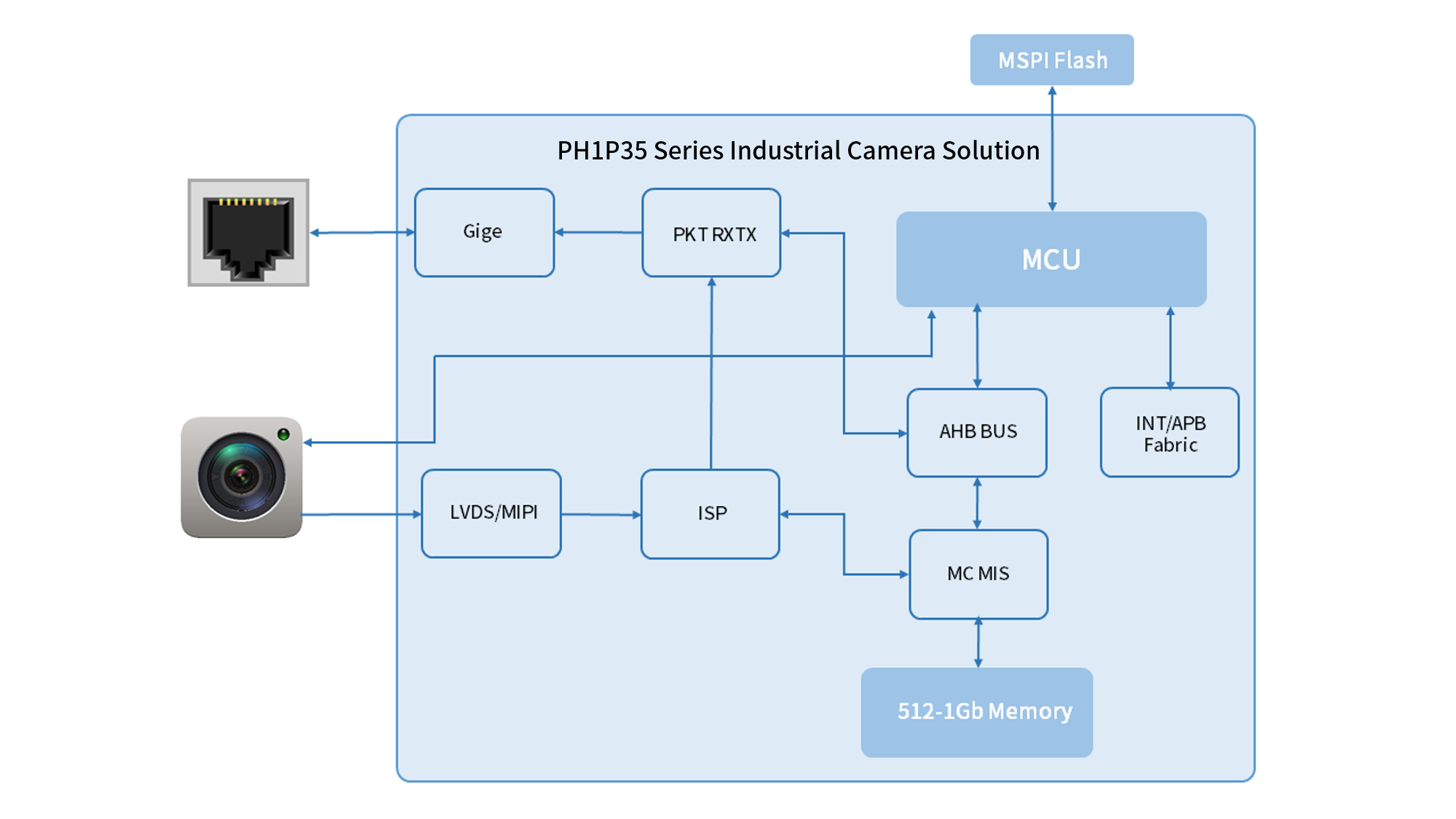
Industrial Camera Solution
Traditional solutions rely on a multi-chip architecture: an independent MCU controls Sensor registers, processes protocols (such as GigE Vision/USB Vision), and responds to upper-computer commands; FPGA implements ISP pipelines, image preprocessing, and high-speed interface management (such as GigE MAC); external DDR chips are used for frame buffering and data processing. The collaboration of multiple chips brings problems such as communication delay, signal integrity, and high power consumption, which become bottlenecks in performance and reliability.
Anlogic PH1P35 innovatively integrates a high-performance FPGA, a hard-core RISC-V MCU, and a large-capacity integrated DDR into one, enabling it to provide customers with a highly integrated single-chip solution with advantages such as high reliability and high performance. This solution is suitable for application scenarios that require high reliability, high performance, and have demands for Sensor control, protocol processing, ISP pipeline, image preprocessing, and high-speed interface management (such as GigE MAC).
Features
1. High-Performance FPGA Core: Abundant Programmable Logic Resources
Flexible implementation for high-speed MIPI CSI-2 and LVDS sensor interfaces;
Real-time ISP image processing pipeline (denoising, correction, enhancement, etc.);
GigE Vision protocol stack (flexibly implemented in logic or MCU);
Customized image preprocessing algorithms (e.g., ROI extraction, simple defect detection).
2. Hard-Core RISC-V MCU: Deeply Integrated, Seamless Cooperation
Efficiently controls Sensor register initialization and configuration (I2C/SPI);
Processes upper-layer software commands and parameter settings (e.g., resolution, exposure time, gain);
Manages device status, performs diagnostics, and supports firmware updates;
Interacts efficiently with FPGA logic to enable intelligent task scheduling.
3. Large-Capacity Integrated DDR:Integrates high-speed DDR memory controller and PHY on-chip, eliminating the need for external DDR chips.
It provides sufficient bandwidth and space for image frame buffering and algorithm data. This significantly simplifies PCB layout and routing, improves signal integrity, and reduces system power consumption and cost.
1. Minimalist Design, Fast Time-to-Market
A single chip replaces MCU + FPGA + external DDR, drastically reducing component count and PCB area;
Simplifies power and clock design, lowers system complexity, and accelerates product development cycles.
2. Remarkable Cost Efficiency and Form Factor Optimization
Save costs on multiple chips and peripheral components;
Reduce PCB layer count and area, lowering manufacturing costs; simplify supply chain management and reduce inventory pressure.
3. Optimized Power Consumption, Green and Energy-Efficient
Eliminate high-speed inter-chip interconnect power;
Integrated DDR delivers higher access efficiency and lower power consumption;
Meet the stringent low-power operation requirements of industrial equipment.
4. Superior Performance, Stability and Reliability
FPGA hard logic implements critical high-speed processing (Sensor interface, ISP, protocol stack) with high determinism and ultra-low latency;
Hard-core MCU ensures real-time and reliable control logic;
On-chip DDR provides a stable high-speed data path;
Simplified design results in fewer failure points and higher system MTBF.
5. Flexible Programmability, Future-Proof
The FPGA’s reconfigurable nature supports Sensor upgrades, algorithm iterations, and protocol evolution. It easily adapts to MIPI/LVDS Sensors with varying resolutions and frame rates, making it convenient for customers to implement differentiated functions and performance optimization.
6. Supply Chain Security
Innovative packaging and process design reduce instability risks associated with multi-device supply chains.
Successful Case Study
A renowned industrial camera brand adopted the Anlogic PH1P35 solution in its new-generation compact GigE Vision camera, successfully achieving:
Reduced PCB size for a more compact camera form factor;
Shortened development cycle to quickly respond to market demands;
Lower overall power consumption and improved thermal control;
Support for 6–8MP Sensors with stable and smooth imaging, earning high recognition from end customers.
As Industry 4.0 imposes higher requirements on vision systems, Anlogic Technology’s PH1P35, with its innovative “FPGA + Hard-Core MCU + Integrated DDR” triune architecture, perfectly addresses core pain points in industrial camera design, achieving all-round breakthroughs in performance, cost, power consumption, size, and reliability. It represents not only a technological innovation but also a key driving force for the industrial vision sector toward a more efficient, intelligent, and convenient future.
Solution Applications
-
 High-Precision Production Line Quality Inspection
Rapidly captures product defects, PH1P35’s high-efficiency processing ensures real-time alerts and improves yield rates.
-
Machine Vision Guidance
Provides precise positioning and recognition capabilities for robotic arms, humanoid robots and so on. The single-chip low-latency feature guarantees fast visual identification and response.
-
Intelligent Logistics Sorting
High-speed recognition of parcel barcodes and shipping label information. The powerful processing capability of PH1P35 meets high throughput requirements.
-
Semiconductor and PCB Inspection
Achieves micron-level precision inspection of components and circuits, with stability and reliability as core guarantees.